The Netherlands, more than just ASML
10/9/2024 11:52:24 AM
The Netherlands, a country famous for tulips and windmills, also enjoys a high reputation in the field of semiconductor equipment. When it comes to the semiconductor industry in the Netherlands, many people first think of ASML, which is well-known for its lithography technology. In addition, there is NXP, a major automotive semiconductor manufacturer. However, perhaps you don't know that in this low-key country, there are many "hidden champions" who focus on niche equipment fields, and they play a vital role in the global semiconductor industry.
ASML, as a treasure of the Dutch semiconductor industry, occupies a pivotal position in the global semiconductor equipment manufacturing field. ASML is the largest exporter in the Netherlands, the largest technology employer in the Netherlands, and the world's largest chip equipment manufacturer. This is mainly because of ASML's lithography machine. As of September 24, 2024, ASML's market value is US$322.9 billion. In 2023, ASML's full-year net sales reached 27.6 billion euros, with a gross profit margin of 51.3% and a net profit of 7.8 billion euros.
Lithography is an indispensable key step in today's chip industry, and advanced lithography machines are known as the "crown jewel" in the integrated circuit equipment manufacturing industry. The lithography machine is mainly responsible for accurately projecting the integrated circuit layout onto the wafer. The lithography machine is a system that integrates precision optics, precision machinery, automatic control and software engineering. It must not only achieve extremely high exposure resolution, but also have extremely high repeatability.
More than 30 years ago, the entire lithography machine market was monopolized by GCA of the United States and Nikon of Japan. Today, 30 years later, there are almost no traces of lithography machines in the United States, and Nikon has fallen behind. On the contrary, ASML's lithography machines are far ahead. From almost nothing in 1984 to growing into the undisputed leader in the lithography machine industry, there are many unknown stories behind ASML.
In the 1980s, ASML started with difficulty. In 1984, electronics giant Philips and chip machine manufacturer Advanced Semiconductor Materials International (ASMI) established ASM Lithography, located in a leaky shed next to Philips' office in Eindhoven, the Netherlands. In the same year, ASML launched its first system, the PAS 2000 stepper. In 1985, ASML had 100 employees and moved into a newly built office and factory in Veldhoven. In 1986, ASML launched the PAS 2500 stepper and established a partnership with Zeiss in the same year. In 1988, Philips began to enter the Asian market after establishing a joint venture factory in Taiwan. However, ASML had few customers and could not be self-reliant. What's worse, shareholder ASMI could not maintain the high investment and decided to withdraw. The situation in the global electronics industry took a sharp turn for the worse, and Philips also announced a large-scale cost-cutting plan. ASML was in danger. Finally, under the persuasion of Philips board member Henk Bodt, he persuaded his colleagues to lend a last helping hand.
In the 1990s, ASML got on track and officially IPOed. In this decade, ASML launched the breakthrough platform PAS 5500, which is also ASML's "longest-lived" lithography system. ASML pointed out that more than 90% of PAS 5500 are still active in production lines in various segments, and their lifespan will be extended to at least 2035. PAS5500 is of great significance to ASML. It helped it gain IBM as a major customer, and made it leap from a startup company less than ten years old to the runner-up in the market in the 1990s. In 1995, ASML became a completely independent public company, listed on the Amsterdam and New York Stock Exchanges. Philips sold half of its shares at the time of its IPO and sold the remaining shares in the following years.
In the 2000s, immersion systems developed rapidly. ASML used immersion technology to significantly improve the resolution of the system and used the revolutionary two-stage TWINSCAN technology to significantly improve production efficiency. In 2003, the industry's first immersion machine, the TWINSCAN AT:1150i, debuted, followed by the TWINSCAN XT:1250i, XT:1400i, and in 2006, the first mass-produced machine for immersion, the XT:1700i. In 2007, ASML launched the TWINSCAN XT:1900i immersion system, which has a numerical aperture of 1.35, the highest in the industry.
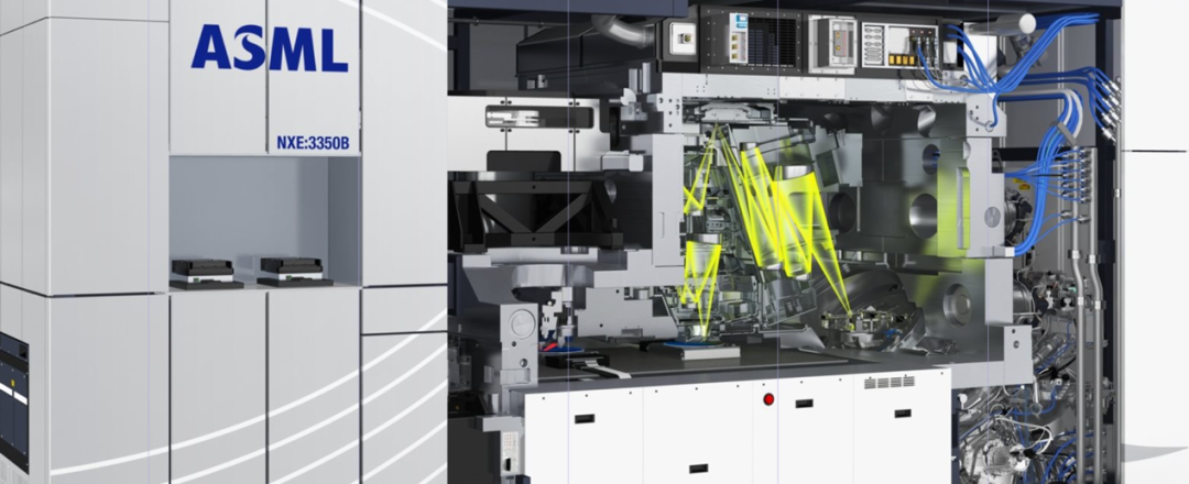
Starting in the 2010s, ASML introduced EUV lithography technology, which once again changed the face of the semiconductor industry. In 2010, the first EUV lithography machine, the TWINSCAN NXE:3100, was shipped to the research institute of an Asian chip manufacturer. The second-generation EUV system NXE:3300 was launched in 2013, and the third-generation EUV system NXE:3350 was launched in 2015. In 2016, EUV lithography technology reached a turning point, and customers began to place orders in bulk for ASML's first production-ready system, the NXE:3400. The NXT1970Ci and NXT1980Di became the main machines in the chip industry.
In fact, in the Netherlands, before ASML, there was an old semiconductor equipment company ASM International NV (abbreviated as ASM), which is the parent company of ASML that we mentioned above, which joined hands with Philips.
ASM was founded in 1968 and has a history of 55 years. ASM initially worked in the furnace deposition market and began producing these equipment in the Netherlands in the early 1970s.
Since then, ASM has continued to expand around the world. In the mid-1970s, ASMPT was established in Hong Kong and became a market leader in back-end semiconductor assembly and packaging equipment. ASM divested its majority stake in ASMPT in 2013, but still retains a minority stake. ASM USA was also founded in the 1970s and now mainly makes epitaxial equipment. In the early 1980s, ASM Japan was established, laying the foundation for today's plasma CVD products. Subsequently, ASM and Philips jointly developed lithography technology in the mid-1980s, which is today's ASML. ASM sold its stake in ASML in 1988.
ASM has operations in 16 countries, so in a sense, ASM is already a global company.
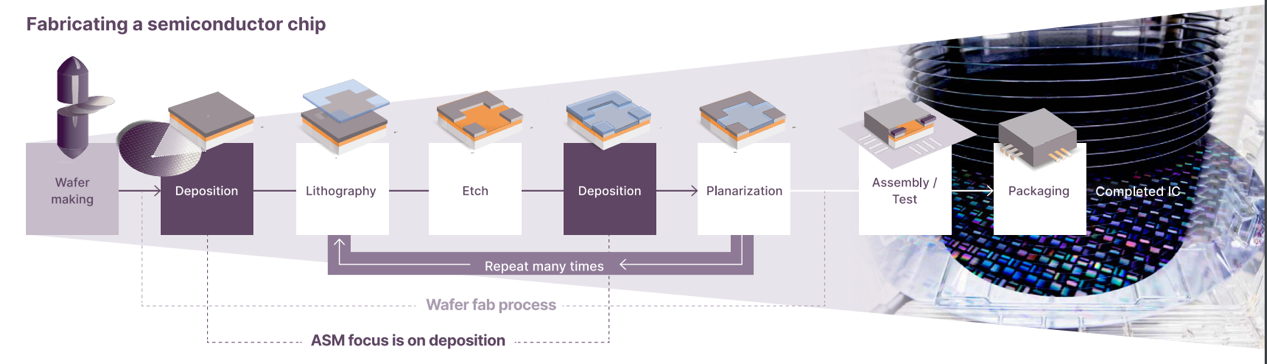
ASM focuses mainly on ALD (atomic layer deposition) and epitaxy. ALD business is ASM's trump card. With more than 55% global market share, ASM is in an absolute leading position in the field of ALD. ALD is the most advanced deposition method on the market, which can produce ultra-thin films with excellent material quality, uniformity and conformality. ALD is also one of the fastest growing segments in the wafer fab equipment market, with an annual average growth rate (CAGR) of 10% to 14% expected between 2022 and 2027.
Silicon epitaxy is ASM's second largest product line, and the silicon epitaxy (Si Epi) business is growing steadily. ASM aims to achieve at least 30% market share by 2025. In recent years, ASM has also occupied a relatively niche market in the vertical furnace and PECVD fields through mergers and acquisitions.
ASM is also a beneficiary of the development of advanced process nodes. ASM's revenue has continued to grow steadily over the past few years, increasing from €1.284 billion in 2019 to €2.634 billion in 2023. Equipment sales accounted for 84% of its revenue, and spare parts and services accounted for 16%.
In the second half of 2023, ASM received important orders for the first batch of GAA trial production line activities. The company believes that GAA is a major turning point for its company. Compared with previous technology nodes, GAA's more complex device architecture will increase ALD's requirements, such as more dipole layers and work function layers. Silicon epitaxy (Si Epi) is also a key technology for GAA, used to build the nanosheets that form the core of transistors.
ASM expects the introduction of 2nm/GAA in high-volume manufacturing (HVM) to significantly drive logic/foundry sales growth in 2025. GAA 2nm technology is expected to enter high-yield manufacturing in 2025 and will become an important driver for ASM. It is expected that by 2027, logic/foundry spending on GAA nodes will account for more than 40% of the total WFE market. And ASM is in an unprecedentedly strong position.
- payment
