Samsung Accelerates Introduction of 1c DRAM Equipment
12/8/2025 10:17:00 AM
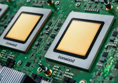
According to a report by DealSite, Samsung Electronics is accelerating the introduction of 10-nanometer-class sixth-generation (1c) DRAM equipment, aiming to begin HBM4 mass production early next year as it strives to catch up with SK Hynix, which has already signed supply contracts with NVIDIA and entered mass production.
Industry sources revealed that Samsung recently completed the installation of 1c DRAM equipment at its second plant (P2) in the Pyeongtaek campus and is simultaneously introducing new equipment at the third (P3) and fourth (P4) plants to actively expand advanced process capacity.
Samsung plans to complete the internal reliability test (PRA) for the final customer sample (CS) this month, after which the sample will be sent to NVIDIA for GPU integration verification. If progress goes smoothly, shipments are expected to begin in the second half of next year. Company insiders stated that after the CS test is completed, NVIDIA will begin a GPU verification process lasting about four months. Once final certification is achieved, Samsung is expected to start allocating mass production orders early next year.
Previously, Samsung's Pyeongtaek P2 and P3 plants mainly produced previous-generation DRAM products. However, as market demand shifts toward high-performance and high-bandwidth applications, the company has gradually reduced production of older process chips and converted part of the lines to the latest 1c process. This transformation involves upgrading existing facilities and equipment to enable older lines to produce next-generation memory chips.
Currently, the fourth plant (P4) is designated as the core production base for HBM4 and is scheduled to begin operations next year. The main fab PH1 is already running both NAND and 1c DRAM production lines; PH3 has been introducing new equipment since June; PH4 is under construction; and PH2 is expected to begin operations at the end of this year or early next year.
Although the 1c process development is progressing steadily, achieving mass-production yield remains Samsung's biggest challenge. Industry sources indicate that current HBM4 samples produced using the 1c process have a yield of around 50%, which has not yet reached the mass production threshold. Because HBM4 adopts a multi-layer stacked structure and larger die area than the previous HBM3E, the number of good chips per wafer decreases, slowing the yield improvement rate.
To address this, Samsung is simultaneously enhancing its back-end packaging process and collaborating with Hanmi Semiconductor to stabilize stacking precision and overall process quality. Analysts note that if Samsung can raise HBM4 wafer yield above 70%, it will meet the conditions for mass production.
The industry widely believes that Samsung's move closely aligns with NVIDIA's schedule for launching its next-generation AI accelerator, Rubin, in the second half of next year. Considering that SK Hynix announced completion of its HBM4 mass production system in September, Samsung's equipment installation and production line conversion are now in the final stages. However, whether the company can achieve stable yield in the short term remains to be seen.
- payment
